Z7-LITE Reference Manual
Development Environment:
Vivado 2018.3 is from Xilinx website
WeChat Public Number:

●1. Overview
Z7 Lite is a commercial-grade development board based on Xilinx Zynq-7000 SoCs (XC7Z010 or XC7Z020) with up to 4Gb of DDR3/L SDRAM, 128MB of SPI flash memory, Gigabit Ethernet PHY transceiver, a USB PHY transceiver and an easy way to support power. With customizable variants available upon request, customised requirements may be subject to minimum order quantities, please contact our sales team for more information: sales@microphase.cn.
It is suitable for software verification and hardware development, helping to accelerate project progress.
○Board Layout

○Key Features
Xilinx Zynq™ XC7Z010-1CLG400C (7010 Version Only),
Xilinx Zynq™ XC7Z020-1CLG400C (7020 Version Only).DDR3: 1 4Gbit,DDR3.(MT41J256M16HA-125:K or equivalent)
KEY: 3 user’s keys, 1 PS control, 2 PL control.
LED: 3 user’s LEDs, 1 PS control, 2 PL control.
GPIO: 2 40 pin expansion ports (2.54mm pitch), 72 IOs of 3.3V voltage.
USB JTAG: 1 on board JTAG circuit, can debug and download the ZYNQ system through the USB cable.
HDMI: 1 HDMI video output interface, can realize 1080P video image.
PHY ETH: 1 10/100 Ethernet RJ45 interface, which can be use for Ethernet data exchange or other application.
USB Host: 1 USB Host.
SD Card: 1 SD Card is provided to store the operating system image and file system.
USB UART: 1 USB UART interface, using for serial communication with PC.
CLOCK: 1 33.33Mhz active crystal oscillator provides a stable clock for the PS system.
1 50Mhz active crystal oscillator provides additional clocks for the PL logic.
○Block diagram

○Mechanical Spec

●2. Function Resources
○FPGA
667 MHz dual-core Cortex-A9 processor
DDR3L memory controller with 8 DMA channels and 4
High Performance AXI3 Slave ports
High-bandwidth peripheral controllers: 1G Ethernet, USB 2.0, SDIO
Low-bandwidth peripheral controllers: SPI, UART, CAN, I2C
Programmable from JTAG, Quad-SPI flash, and microSD card
Programmable logic equivalent to Artix-7 FPGA
LUTs: 17,600 (7010)
53,200(7020)
DSP Slices: 80 (7010)
220 (7020)
Logic Cells: 28K (7010)
85K(7020)
Flip-Flops: 35,200 (7010)
106,400 (7020)
Total Block RAM: 2.1Mb (7010)
4.9Mb (7020)Analog Mixed Signal (AMS) / XADC: 2x 12 bit, MSPS ADCs with up to 17 Differential Inputs
Security: AES & SHA 256b Decryption & Authentication for Secure Programmable Logic Config
○DDR3
One on-board 16bit 512M DDR3/L SDRAM chips.
| Position | Model | Capacity | Factory |
|---|---|---|---|
| U4 | MT41K256M16 | 256M x 16bit | Micron |
| Signal Name | PIN Number | Signal Name | PIN Number |
|---|---|---|---|
| PS_DDR3_A0 | N2 | PS_DDR3_D0 | C3 |
| PS_DDR3_A1 | K2 | PS_DDR3_D1 | B3 |
| PS_DDR3_A2 | M3 | PS_DDR3_D2 | A2 |
| PS_DDR3_A3 | K3 | PS_DDR3_D3 | A4 |
| PS_DDR3_A4 | M4 | PS_DDR3_D4 | D3 |
| PS_DDR3_A5 | L1 | PS_DDR3_D5 | D1 |
| PS_DDR3_A6 | L4 | PS_DDR3_D6 | C1 |
| PS_DDR3_A7 | K4 | PS_DDR3_D7 | E1 |
| PS_DDR3_A8 | K1 | PS_DDR3_D8 | E2 |
| PS_DDR3_A9 | J4 | PS_DDR3_D9 | E3 |
| PS_DDR3_A10 | F5 | PS_DDR3_D10 | G3 |
| PS_DDR3_A11 | G4 | PS_DDR3_D11 | H3 |
| PS_DDR3_A12 | E4 | PS_DDR3_D12 | J3 |
| PS_DDR3_A13 | D4 | PS_DDR3_D13 | H2 |
| PS_DDR3_A14 | F4 | PS_DDR3_D14 | H1 |
| PS_DDR3_BA0 | L5 | PS_DDR3_D15 | J1 |
| PS_DDR3_BA1 | R4 | PS_DDR3_DQS_N0 | B2 |
| PS_DDR3_BA2 | J5 | PS_DDR3_DQS_N1 | F2 |
| PS_DDR3_NCAS | P5 | PS_DDR3_DQS_P0 | C2 |
| PS_DDR3_CKE | N3 | PS_DDR3_DQS_P1 | G2 |
| PS_DDR3_CLK_N | M2 | PS_DDR3_NRST | B4 |
| PS_DDR3_CLK_P | L2 | PS_DDR3_ODT | N5 |
| PS_DDR3_NCS | N1 | PS_DDR3_NRAS | P4 |
| PS_DDR3_DM0 | A1 | PS_DDR3_NWE | M5 |
| PS_DDR3_DM1 | F1 |
○Giga ETH
The RTL8201F chip supports 10/100M network transfer rate and communicates with the MAC layer of the Zynq7000 PS system via the RGMII interface. It supports MDI/MDX adaptation, multiple speed adaptation, master/slave adaptation and MDIO bus support for PHY register management.
○USB Host
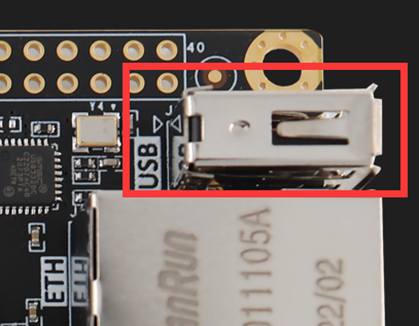
The USB2.0 transceiver on-board is the USB3320C-EZK, which is supports the ULPI standard interface. It’s connected with ZYNQ’s bus interface to enable high-speed USB2.0 Host mode data communications.
○USB UART
A USB to UART chip, the CH340, is provided for user connection to the host PC.
| Signal Name | Pin Name | Pin Number | Explain |
|---|---|---|---|
| UART_TX | PS_MIO15_500 | C8 | UART data output |
| UART_RX | PS_MIO14_500 | C5 | UART data input |
○USB JTAG
We have incorporated the JTAG download and debug circuitry into the board, enabling users to develop and debug ZYNQ through a USB cable.
○Boot Config
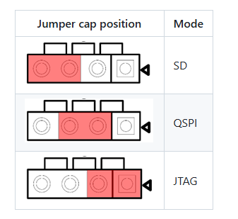
The Z7-Lite startup settings include JTAG, QSPI and SD modes, which are controlled by the MODE input signal from the J1. The user has the option to change mode through the jumper cap. The startup mode is configured as shown in the figure below.
○Quad-SPI Flash
The onboard 128M Quad-SPI Flash memory W25Q128JVSIQ is used for the storage of the initial FPGA configuration, user applications and data.
| Position | Model | Capacity | Factory |
|---|---|---|---|
| U2 | W25Q128JVSIQ | 128M Byte | Winbond |
○Clock
A 33.33 MHz active crystal oscillator provides a stable clock for the PS system, while the other 50 MHz active crystal oscillator provides additional clocks for the PL logic.
| Position | Signal Name | Frequency | Pin Number |
|---|---|---|---|
| Y1 | PS_CLK_33d3 | 33.333Mhz | E7 |
| U3 | PL_CLK_50M | 50Mhz | N18 |
○Reset
We provide a key (K1) that can be used as a ‘reset’ signal for designs running on FPGA.
○Micro SD
The board provides a Micro SD card interface, allowing users to access the SD card memory. It also provides storage for the ZYNQ chip’s bootloader, Linux operating system kernels, file systems, and other user data files.
○HDMI
One HDMI video output interface can realize 1080P video images.
○LED
We provide three LEDs for user to use. When the corresponding pin of the FPGA is in a low state, the LED is illuminated.
| Position | Signal Name | Pin Number | Explain |
|---|---|---|---|
| D3 | PS_LED1 | E6 | PS LED1 |
| D4 | PL_LED1 | P15 | PL LED1 |
| D5 | GPIO1_17N | U12 | PL LED2 |
○Key
We provide three keys for user to use. Once the key is pressed, it will be on the low level.
| Position | Signal Name | Pin Number | Explain |
|---|---|---|---|
| K2 | PS_KEY1 | B5 | PS KEY1 |
| K3 | PL_KEY1 | P16 | PL KEY1 |
| K4 | GPIO1_17P | T12 | PL KEY2 |
○GPIO
This device is equipped with a maximum of 72 user IO pins that can be used for various custom applications. All user IOs are length matched and can be used as differential pairs.
JP1:
| Pin | Signal Name | Pin Number | Pin | Signal Name | Pin Number |
|---|---|---|---|---|---|
| 1 | GPIO1_0P | N17 | 2 | GPIO1_0N | P18 |
| 3 | GPIO1_1P | R16 | 4 | GPIO1_1N | R17 |
| 5 | GPIO1_2P | T16 | 6 | GPIO1_2N | U17 |
| 7 | GPIO1_3P | W18 | 8 | GPIO1_3N | W19 |
| 9 | GPIO1_4P | Y18 | 10 | GPIO1_4N | Y19 |
| 11 | VCC_5V | - | 12 | GND | - |
| 13 | GPIO1_5P | Y16 | 14 | GPIO1_5N | Y17 |
| 15 | GPIO1_6P | V17 | 16 | GPIO1_6N | V18 |
| 17 | GPIO1_7P | W14 | 18 | GPIO1_7N | Y14 |
| 19 | GPIO1_8P | V16 | 20 | GPIO1_8N | W16 |
| 21 | GPIO1_9P | T17 | 22 | GPIO1_9N | R18 |
| 23 | GPIO1_10P | V12 | 24 | GPIO1_10N | W13 |
| 25 | GPIO1_11P | T14 | 26 | GPIO1_11N | T15 |
| 27 | GPIO1_12P | T11 | 28 | GPIO1_12N | T10 |
| 29 | VCC_3V3 | - | 30 | GND | - |
| 31 | GPIO1_13P | V15 | 32 | GPIO1_13N | W15 |
| 33 | GPIO1_14P | P14 | 34 | GPIO1_14N | R14 |
| 35 | GPIO1_15P | U14 | 36 | GPIO1_15N | U15 |
| 37 | GPIO1_16P | U13 | 38 | GPIO1_16N | V13 |
| 39 | GPIO1_17P | T12 | 40 | GPIO1_17N | U12 |
JP2
| Pin | Signal Name | Pin Number | Pin | Signal Name | Pin Number |
|---|---|---|---|---|---|
| 1 | GPIO2_0P | L16 | 2 | GPIO2_0N | L17 |
| 3 | GPIO2_1P | H15 | 4 | GPIO2_1N | G15 |
| 5 | GPIO2_2P | F16 | 6 | GPIO2_2N | F17 |
| 7 | GPIO2_3P | E18 | 8 | GPIO2_3N | E19 |
| 9 | GPIO2_4P | B19 | 10 | GPIO2_4N | A20 |
| 11 | VCC_5V | - | 12 | GND | - |
| 13 | GPIO2_5P | D19 | 14 | GPIO2_5N | D20 |
| 15 | GPIO2_6P | E17 | 16 | GPIO2_6N | D18 |
| 17 | GPIO2_7P | H16 | 18 | GPIO2_7N | H17 |
| 19 | GPIO2_8P | G19 | 20 | GPIO2_8N | G20 |
| 21 | GPIO2_9P | J18 | 22 | GPIO2_9N | H18 |
| 23 | GPIO2_10P | K16 | 24 | GPIO2_10N | J16 |
| 25 | GPIO2_11P | C20 | 26 | GPIO2_11N | B20 |
| 27 | GPIO2_12P | G17 | 28 | GPIO2_12N | G18 |
| 29 | VCC_3V3 | - | 30 | GND | - |
| 31 | GPIO2_13P | L19 | 32 | GPIO2_13N | L20 |
| 33 | GPIO2_14P | F19 | 34 | GPIO2_14N | F20 |
| 35 | GPIO2_15P | M19 | 36 | GPIO2_15N | M20 |
| 37 | GPIO2_16P | K19 | 38 | GPIO2_16N | J19 |
| 39 | GPIO2_17P | J20 | 40 | GPIO2_17N | H20 |
○Power
The board uses a +5V supply from USB. The Figure shows the USB can be used to provide power.
